
Iran-China
Virtual Symposium
on
Nanoscience and Nanotechnology
Speech Details
Official collaborations in science and technology, especially on Nanotechnology, have been recently initiated between Iran and China. Many effective programs have been launced in this regard, such as the joint program by Iran vice presidency for science and technology and China Academy of Science (CAS). This event aims to initiate and promote scientific collaboration between Iranian and Chinese scientists. We propose to organize and run this event by the consortium of 5 top Iranian Universities of Technology (UT5), in order to facilitate direct contact of the leading scientists of these universities with their Chinese counterpart. Furthermore, in this event a special program to introduce Iranian startup companies in this field to Chinese Technoparks and investment agencies is considered. We propose that the yearly event of NanoIRCN to be held virtually in 2021, and be continued in the consecutive years in Iran and China.
Speakers

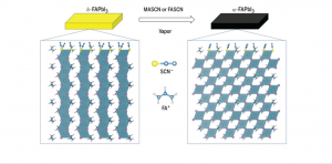
Highly efficient and stable black phase FAPbI3 perovskite solar cells
Abstract. Metal-halide perovskite which has the structure of ABX3, has become one of the most intensively studied optoelectronic materials, especially in the application of solar cell. Most of the perovskite solar cell with high efficiency are based on the mixed A cations or X ions. However, this comes at the cost of long-term stability, due to the loss of volatile methylammonium and phase segregations. It has been reported that the α-FAPbI3 has the ideal cubic crystal structure, and lower band gap compared to mixed cation perovskite. However, the black α-FAPbI3 is unstable at room temperature, easy to transform to photo inactive δ-FAPbI3. Therefore, obtaining efficient and stable FAPbI3 PSCs is of vital importance for the perovskite research field. Here, we report a novel sequential deposition method employing MASCN vapour treatment of yellow phase FAPbI3 perovskite films for making highly crystallized, pure black phase FAPbI3 PSCs and achieve a power conversion efficiency up to 23.5%. We attain a high open-circuit voltage (VOC) of 1.18 V corresponding to a loss of only 300 meV with respect to the band gap energy of 1.48 eV setting a new record in the whole PV field.
-
Lu, H. Z. et al. Vapor-assisted deposition of highly efficient, stable black-phase FAPbI(3) perovskite solar cells. Science 370, 74-+, eabb8985 10.1126/science.abb8985 (2020).
Title: Linking Thermoelectric Generation in Polycrystalline Semiconductors to Grain Boundary Effects Sets a Platform for Novel Seebeck Effect-Based Sensors
Abstract:
Data available on the thermoelectric properties of polycrystalline semiconductors are inconsistent, riddled with gaps, and ascribe stronger Seebeck effects to polycrystalline samples rather than single crystals without explanation. Here, we demonstrate that a grain boundary positioned perpendicular to the applied temperature gradient contributes significantly to the Seebeck voltage generation in the sample, elevating its Seebeck coefficient. This contribution is analytically linked to the height and width of the energy barrier experienced by charge carriers diffusing from one grain to the next. These are primarily extrinsic properties and can be affected by external physicochemical parameters. Occurrence of chemo- and piezo-thermoelectric effects are analytically predicted. Experimental results on SnO2 and ZnO samples with different nanostructures verify the predictions. The presented model sets a novel platform for designing a range of Seebeck effect-based sensors, and unveils the potential of the polycrystalline semiconductors with appropriately designed intergranular regions as thermoelectric materials.


Title: Plastic Deformation Induced Nanocrytstallization
Abstract:
Vapour deposition, plasma processing, gas-condensation, chemical precipitation and crystallisation from the amorphous phase are well established processing routes for obtaining nanocrystalline materials. However, it is well known that mechanical deformation, as a top-down solid-state synthesis route, can also be applied for production of a nanocrystalline structure. Comparison of different preparation methods in terms of cost and productivity demonstrates that mechanical deformation is the most cost effective route capable of producing nanocrystalline materials in large quantity. Grain refinement to the nanometre size is governed by the plastic deformation induced during mechanical working. In general, the grain/crystallite size decreases continuously with number of deformation cycles until a minimum (saturation) size is approached. Further refinement seems to be difficult to achieve for a fixed set of experimental conditions. In this talk the most relevant features of different techniques for producing nanocrystalline materials based of mechanical deformation are overviewed and discussed.
Title: Controllable Nano Oxide Particles and Application Technologies Research Progress in Centre for Nanoscience and Technology, Shanghai University
Abstract:
Nano oxide particles can be widely applied to such fields as electronic ceramics, functional coatings, personal care products, environmental catalysis, advanced batteries, and precision polishing. This report gives brief introduction of relevant research progresses at Research Centre for Nanoscience and Technology, Shanghai University, in the aspects of controllable preparation, surface modification and stable dispersion technology development of nano oxide particles, with also introduction of industrialization base construction for nano oxide particles, as well as their applications in hybrid functional coatings, oil drilling fluids, air purification, electronic functional ceramics, sunscreen cosmetics and lithium-ion batteries.


Title: Innovation and Commercialization: Nanotechnology Industry in Suzhou Industrial Park
Abstract:
Established in 1994, Suzhou Industrial Park, short for SIP, is the flagship cooperation project between Chinese and Singaporean governments. The last two decades have seen SIP rising to one of the top stars regarding the economic strength and innovation vitality in the course of China’s opening-up and reform. Entering into the 21st century, the local government rolled out a new development strategy for industrial and economic transformation and upgrading, and Nanotechnology Industry was then chose as one of the new driving forces accompanied by series of tangible moves such as setting up a managing entity, building up an industrial park for nanotechnology innovation and commercialization and formulating supportive policy to lure elites and STEM experts. Ms. Jane WU’s short introduction will help give a glimpse to the developing status of the city and nanotechnology industry with the hope of generating possible connection and cooperation with other distinguished experts and institutions participating in the summit.
Title: Design and fabrication of monolithic catalyst for plasma-catalytic oxidation of toluene
Abstract
As one of the promising techniques for the abatement of Volatile organic compounds (VOCs), non-thermal plasma (NTP) technique has been attracting close attention recently due to its low temperature, convenient start-up and shutdown procedures, its low-cost, and being applicable to a wide range of VOCs. The synergetic positive effect between plasma and catalysis would be a key to improve efficiency and decrease the energy consumption. Honeycomb monolith catalyst gives lower pressure drop across the reactor compared with the packed-bed reactor. However, the generation of plasma might be suppressed by the separated channel walls between the two electrodes. In this sense, the monolithic catalyst with designed pore structure might solve this problem. Recently, we tried to use foam-like monolithic catalyst which might combine both the advantages of low pressure drop and plasma generation due to the open pore structure, and, therefore, it would be worthwhile to be investigated. We demonstrated that copper foam is an effective monolithic support to support one dimensional CuO nanowires and Mn-Co compounds in a dielectric barrier discharge (DBD) non-thermal plasma reactor for the oxidation of toluene. The shape of copper foam could be tailored to the desired cylindrical form to fit the DBD reactor. were facilely in-situ grown on the surface of the copper skeleton as active components, through a heating process and a followed dip-coating process. The abatement of toluene was applied to evaluate the performance of such a monolithic copper foam in the combined plasma–catalytic process. In addition, material extrusion additive manufacturing is also being applied to design different porous structures for VOC abatement via NTP.


Title: Controllable preparation, dispersion and application of highly dispersed nanoparticles
Abstract:
Nanoparticles have excellent optical, electrical and mechanical properties, etc., and are widely used in photoelectric conversion, new materials and other fields. The dispersion and stability of nanoparticles are the key problems that restrict their application. Our team has studied a series of controllable preparation, surface control, dispersion and stabilization methods of nanoparticles. First of all, according to the “bottom-up” strategy, by controlling the nucleation process and crystal growth process from molecules to nanoparticles, we can finely control the crystal form, morphology and size of nanoparticles. Secondly, based on the stabilization mechanism, we study the surface modification of nanoparticles and the stabilization methods in different solvent systems and high solid content conditions. Then, the applications of highly dispersed nanoparticles in functional composites, injection reagent in oilfield and other fields were investigated.
Title: Nanotechnology at the interface of 3D printing and Bio-engineering
Abstract
One main issue in the perfect and better to say expected fulfilment and implementation of nano-science and thereof advantages in nano-based products and technologies is the exploitation of nano-events when unique properties of nanomaterials or/and nano-structures come into matter. One of the areas of nanotechnology with increasing interest among researchers and industries falls at the common borders of bio-based polymeric nanocomposites processed via advanced technologies such as 3D printing. However, first of all, the fabrication techniques addressing perfect distribution/dispersion of nanomaterials within the polymeric matrix resulting in homogeneous bulk specimens are of high importance whilst still ongoing challenges need to be overcome. The issue is even more highlighted in the case of emerging technologies of 3D printing techniques mainly introduced in design and development of bio and tissue engineering parts. Therefore, it seems the technology of 3D printing is somehow lagging behind the nano and bio-composite science in some points of view specifically when novel nano/bio materials are to be incorporated in bio-based matrices. Above this, in technologies such as fused deposition modeling (FDM) filaments with limited composition available cannot be even appropriately close to what researchers desire in fabrication of bio-based parts including tissue scaffolds or implants reinforced with nano/bio phases with drug delivery characteristics. Moreover, nanocomposite filaments of desired flexibility/toughness are not always fulfilled using conventional extrusion techniques, which, in turn, limits their FDM processing. This talk starts with a brief introduction to conventional methods of nanocomposite fabrication with particular concentration on nano-materials dispersion mechanisms followed by a focus on direct 3D printing technology in the development of polymeric nanocomposites utilizing a rather novel 3D printing method when the need for the filaments is eliminated. We will discuss how the direct 3D printing addresses stumbling block issues in nano and bio material dispersion within polymeric matrices where a broader range of matrix phases and nanomaterials meets researchers needs in design of bio- and nano engineered parts at the interface of nano and 3D printing technologies.


Role of Nanostructures in Improving Solar-driven Photoelectrochemical Water Splitting to Produce Hydrogen
Abstract:
With increasing the world population and rise in energy demands from one side and severe environmental impacts (i.e. the release of CO2 and other contaminants produced by the widespread use of finite fossil fuels) from other side, extensive efforts have been devoted by many researchers in the last two decades to develop efficient technology for generating a clean and renewable source of energy which is pivotal for future carbon-free society. Photoelectrochemical (PEC) solar water splitting on an appropriate semiconductor (SC) catalyst to produce hydrogen is one of the most ideal strategies because it requires only water and sunlight (1). But, solar to hydrogen (STH) conversion efficiency is quite low, due to some intrinsic limitations such as bandgap energy, carrier lifetime, diffusion distance and photostability of a semiconductor examine in the process. In addition, slow charge transfers at the electrode/electrolyte interface and fast recombination of electron-hole pairs limit the PEC reaction rate. The emergence of nanomaterials with adjustable shapes and dimensions ensure progress in PEC/photocatalytic (PC) water splitting. Thus, it is necessary to use nanostructured materials with high surface to volume ratio that facilitate charge separation and suppress electron-hole pair recombination rate. Suitable materials focused mainly on the development of semiconductors that have band gap energy in the visible range of solar spectrum such as Fe2O3, BiVO4, WO3 and CdS. Moreover, three classes of 2D materials including graphene, transition metal dichalcogenides (TMDs), and graphitic carbon nitride (g-C3N4) with remarkable electronic and optical characteristics as well as their main roles in the photoelectrocatalytic production of hydrogen are discussed. Combined 2D layered materials interfaced with other SCs can markedly enhance the PEC/PC efficiencies via band gap alteration and heterojunction formation. The lecture addresses all these issues and introduce several methods to chemically modify nanostructures for achieving efficient photoelectrochemical water splitting towards hydrogen generation. But due to massive strain on freshwater resources globally (about 97 % of the entire world’s water resources is present in the sea), it is an ideal to study PEC by using seawater splitting process. Some aspects related to solar driven direct seawater splitting to hydrogen and oxygen will be described by introducing several high-performance nanostructured catalysts with abundant active sites and corrosion resistance in saline electrolyte. Finally, kinetics and mechanism of the PEC reaction will be discussed in the presence and absence of light for better comparison.


Nanofiber-Based Stretchable Electronics and Power Harvesting Devices
Abstract:
This talk is mainly focused on scientific strategies to integrate electronic devices into nanofibers and textile materials. Wearable electronics fabricated on lightweight and flexible substrate are widely believed to have great potential for portable devices. Several promising applications, for example e-skin, smartwatches, and bracelets, have been successfully achieved for the replacement of conventional electronic gadgets. Lightweight and wearable power supply modules with high energy storage performance are desirable for wearable technology. One strategy is to directly integrate a conventional rechargeable energy storage device, such as a battery or a supercapacitor (SC), into fabrics. Also nanochemistry is an emerging sub discipline of the chemical and materials sciences that deals with the development of methods for synthesizing nano scale bits of a desired material and with scientific investigations of the nano material obtained.
Nano materials have numerous possible commercial and technological applications including use in electronic. In the last few decades, there has been significant progress in one-dimensional (1D) nanostructures with nanoscale and molecular scale properties that can satisfy the demands of the 21st century, for example, carbon nanotubes, inorganic semiconducting and metallic nanotubes/wires, conjugated polymer nanofibers/tubes, etc. These nanostructures have a deep impact on both fundamental research and potential applications in nanoelectronics or molecular electronics, nano devices and systems, nanocomposite materials, bio-nanotechnology and medicine.
Iran experience in implementing a comprehensive nanotechnology development plan
Abstract:
Catching up in advanced emerging technologies is a key factor for developing nations to take an active role in technical aspects and also secure a share in emerging future markets. This is particularly the case for nanotechnology as a platform technology which is diffusing in all industrial sectors and will touch all aspects of the human life in future. This includes the health sector which has already experienced major developments as a result of application of new nanotechnologies. Developing countries due to their limited resources need to carefully devise their national plan and follow some delicate strategies in this regard. Based on her fourth 5-year national economic development plan, Islamic Republic (IR) of Iran has set nanotechnology as one of its top priorities. In this respect, in 2005 Iranian government formally initiated a 10-year “Nano Initiative Plan” developed by Iran Nanotechnology Innovation Council (INIC) followed by the 2nd 10-year plan (2015-2025). The council is responsible for policy making, supporting nanotechnology activities in the whole value chain, and supervising and assessing the outcome of the implemented program. The main target of this program is to create wealth and improve quality of people’s life through application of nanotechnology. As a result of a comprehensive capacity building program, at the moment, more than 69 universities are providing nanotechnology MSc and PhD degrees and total number of post-grad students studied in these universities has exceeded 37000. Regarding science generation, in 2020, Iran was ranked 4th amongst active countries in this field by publishing more than 10000 ISI papers. Regarding industrial achievements, more than 300 start up and manufacturing companies have already introduced their products in the market and exported to more than 45 countries. Currently there are more than 720 nanotechnology certified products and tools in the market developed by these enterprises. Among them there are many health related products including anticancer medicines benefiting from targeted delivery nanotechnologies, cancer detection nano-biosensors, and cosmetic products. Further, INIC to support commercialization of the manufactured nano products, have also actively been involved in publishing 121 national and 8 international (ISO/TC229) nanostandards as well. It worth to mention that industrial nanotechnology developments have been accompanied with appropriate environmental and health considerations. As an example, Iran Nanosafety Network can be mentioned which was established in 2012 with the aim of networking experts active in this field and supporting the sustainable and safe production of nano products in Iran. In addition specialized committees have been established in the ministry of health, ministry of agriculture and veterinary organization. Iran’s achievements in nano-based health products not only contributed to economic output but also have directly affected people’s quality of life.

Phosphorene nano sheets and nanostructures and their applications towards the fabrication of high performance field effect transistors
Abstract:
Phosphorene nanosheets are among the few elemental two-dimensional materials with a direct band gap which is tunable with the thickness of the constituting layers. In this presentation, the superior performance of field effect transistors which have been realized using phosphorene nanosheets on silicon substrates are presented. The growth of P-S is achieved by the deposition of an amorphous red phosphorus on silicon or other substrates and further plasma or laser treatment to convert the amorphous film into a highly crystalline 2D sheets. The evolution of single crystalline regions with sizes up to 500 micrometers is reported. The growth parameters can be adjusted to arrive at single or few layered features with ability to be applied for the fabrication of field effect transistors. We have successfully realized transistors with high values of mobility up to 1000 cm2/Vs and a relatively good on-off ratio of 1000. Apart from their electrical behavior, we have studied and report their optical properties. In addition, we have observed exciting new findings on the interactive of biomolecules such as Cysteine amino acid with the exposed phosphorous atoms on the surface of the phosphorene sheets. This material, functionalized with bio-molecules has a promising opportunity for bio-sensors with high sensitivity and low toxicity. We are also working on the fabrication of a corona-sensing device using bio-activated sheets.
Organic Nanostructures for Flexible Solar Cells and Energy Storage Devices
Abstract:
Recently, nanostructures of functional polymers were found to be particularly advantageous for energy conversion and storage, which will lead to a promising application in flexible electronic devices. We are focusing on the energy conversion and storage for wearable electronics, including organic solar cells and energy storage devices. For organic solar cells, we introduced a ternary systems containing two donors and one acceptor (or one donor and two acceptors). The ternary strategy is important for optimizing the morphology of organic solar cells, and therefore can improve the performance of printed flexible devices. For flexible energy storage devices, a facile one-step approach to prepare vertically aligned nanostructure arrays on various substrates was introduced. Flexible energy storage devices were further demonstrated, which possessing the merits of large capacitance, high rate capability and good stability.
